Using Simulation and Modeling for medical Radio Frequency design
A study demonstrating the benefits of simulation over prototyping
Newsletter EnginSoft Year 18 n°2
By Enrico Denna | Flex
Enrico Denna is Hardware Engineering Manager at Flex
Enrico Denna is Hardware Engineering Manager at Flex
The growth of technology and end-user expectations is ever more important in many application areas and medical devices are at the forefront of this innovation process.
The requirements of an even more connected world have had a significant impact on electronic design and specifically on the area of radio frequency (RF) which by
its very nature represents a major design challenge. Modeling and simulation are valid instruments to assist in achieving this goal because performance
in electromagnetic design cannot be easily predicted in advance by relying solely
on the experience of the designer.

CASE STUDY
A fascinating article on the origin, history, and evolution of roller coasters from their earliest prototypes in Russia in the 16th century on the banks of the Neva River of St. Petersburg, and then dives into detail on how numerical simulation of roller coasters works to ensure their success both as entertainment and from a safety perspective for users and operators.
mechanics civil-engineering construction optimization
CASE STUDY
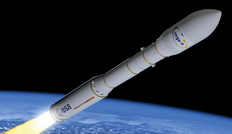
This article is based on a collaboration between RBF Morph and AVIO to configure a numerical optimization procedure to improve the Vega E M10 engine’s performance by optimizing the methane circuit of the injector head.
aerospace rbf-morph ansys meshing